After all the TT7F flights sent their last messages and descended back to ground somewhere around the world, I thought about what interested me the most at that point. The answer was that I wanted to know more about their fate. What led to their departures and whether there was something that could have been done better. In light of that, I decided to make a data oriented tracker designed to collect and deliver as much data on the balloon's behaviour as possible. This blog post is intended to document the whole process - the planning, designing and manufacturing of TT7B (B stands for balloon) superpressure balloon tracker. The basic ideas were:
- powered by a single AAA primary cell to provide overnight operation
- developed around low power components allowing 1.8V operating voltage
- equipped with temperature and pressure sensors to report on conditions inside and outside of the balloon
- sufficient amount of non-volatile memory for extended backlogging
- only geofenced APRS transmissions
- low duty cycle to extend the battery life
- minimum mass to not add too much to the fixed mass of the primary cell
The APRS transmissions are short enough not to waste too much power. The coverage around the world is sufficiently predictable to further save power by limiting the transmissions to areas with active receivers only. The backlogging will fill in the data for when the tracker is out of reach should the balloon survive to the next receiver hotspot. The data might provide insight into the balloon's behaviour during its ascent, the day-night cycle, and potentially its descent as well.
There is an enormous number of ICs, passive components, sensors and so on available on the market. I usually use the online catalogues of large distributors like Mouser or Farnell to search through all the different options. They often provide a lot of the information at hand including the cost, and simplify the search for what one is after.
Most of the information, though, can be found in a component's datasheet. These often tens or hundreds of pages long documents are usually linked to from the catalogues. If not, a quick google search will most likely fetch it among the top results. These pdf files then contain detailed specification of the component, requirements on basic wiring, examples of application, recommended PCB mounting, etc. With the basic concept in mind, I started choosing individual parts and outlining a schematic.
Microcontroller
The microcontroller is the main middleman that needs to be equipped to be able to interface with all the other parts. It is also the component that will run continuously, hence its consumption is a factor to be taken into account. Due to its low power performance and my familiarity with the Atmel/Microchip environment, the 32 pin Cortex M0+ SAML21E series of MCUs was chosen to be in the middle of the tracker. There are a few pin compatible variants: E15, E16, E17 and E18 which differ in SRAM and flash memory sizes. The 128kB flash and 32kB SRAM version, E17, seems like the best compromise between its cost and memory size for my objective. Its datasheet provides a basic check list on what needs to be done to make a custom implementation work. The schematics and user guide of SAML21 Xplained Pro evaluation board are a useful source of information as well.

Starting with the power supply, VDDIN and VDDANA are supplied with 1.8V. Both require a 10µF decoupling capacitor at the input and a 100nF capacitor as close to the pin as possible for filtering high frequency noise in the power supply. VDDANA serving as an analog reference is further filtered with a ferrite bead (BLM15PX471SZ1D - Z=470Ω (at 100MHz), Rdc=0.65Ω, Imax=1A). The MCU is equipped with an internal regulator for its core. The regulator can be run in Low Power mode in case of standby and either a Linear or a more efficient Switching mode when active. The Switching mode, however, requires a large inductor between VSW and VDDCORE pins. I've chosen the simpler Linear implementation for the tracker with only two external decoupling capacitors (1µF and 100nF) at VDDCORE leaving the Switching mode regulator output VSW unconnected.
A post by Bristol SEDS on their
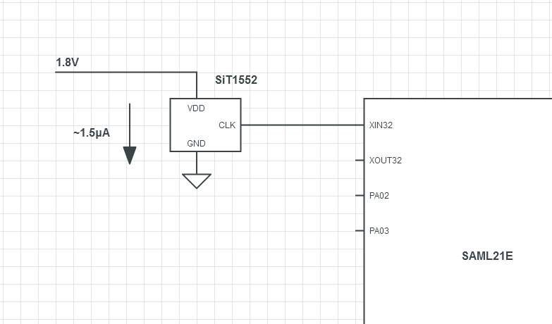
UBSEDS13 tracker informed me about the existence of very low power 32.768kHz TCXOs that can be used to provide a clock signal to a microcontroller. This temperature stable signal then serves either directly or as the basis for the MCU's internal clock generators which provide higher frequency programmable clocks to individual domains. There are a few versions of the SiT1552 TCXO differing in their output. I've chosen the LVCMOS version that is specced as minimum high at 90% of VDD, maximum low at 10% of VDD with 48-52% duty cycle which is in compliance with the XOSC32K Digital Clock Characteristic in the MCU's datasheet. The clock signal is fed to XIN32 pin while XOUT32 is left unconnected. The datasheet also recommends leaving PA02 and PA03 as 'static' as possible, so they won't be utilized in the design. The other crystal input pins XIN and XOUT are used as general I/O pins. The TCXO will be powered continually with expected ~1.5µA. The consumption of the MCU itself depends on a number of factors and settings. According to the datasheet it typically moves around 60-95µA/MHz in active mode and down to 1.2µA in standby mode.
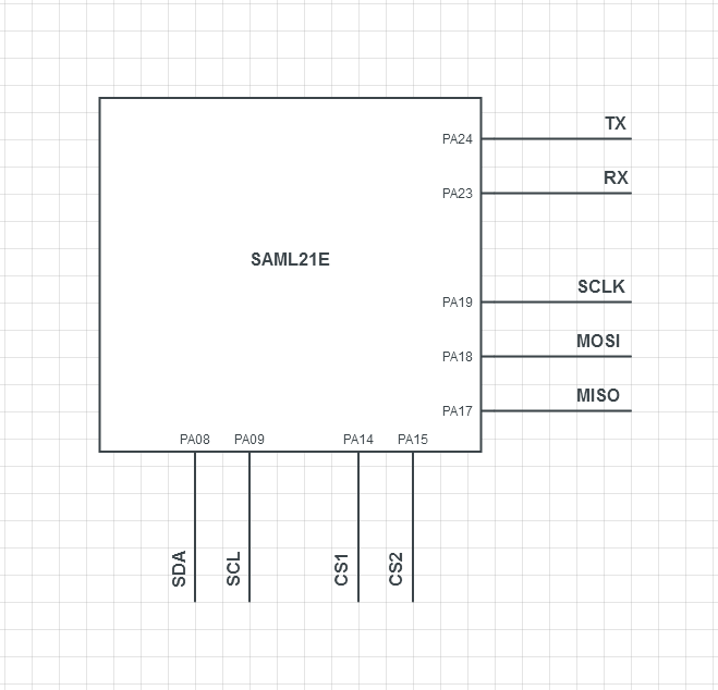
The tracker will utilize all three serial interfaces. UART for communication with a GPS module, I
2C for a link to a transmitter and an ambient light sensor, and SPI to command two pressure sensors. There are six instances of SERCOM peripheral in the MCU and each can be configured to support one of the interface modes. There are four pads per SERCOM instance multiplexed with general purpose pins all around the IC. Each interface allows some degree of freedom in choosing which signal will be present on which pad. I've selected the pins as can be seen in the illustration above taking into account the eventual layout of the board. I
2C's SDA and SCL signals are on pads 0 and 1, respectively, of SERCOM 0 or 2. SPI's MISO, MOSI and SCLK on pads 1, 2 and 3 of SERCOM 1 or 3. The two chip select (slave select) pins have to be controlled manually, and as such are placed on general purpose pins PA14 and PA15. UART's RX and TX signals are then on pads 1 and 2 of SERCOM 3 or 5.
Three ADC inputs and one DAC output had to be allocated among the remaining pins. Both the ADC and DAC peripherals provide 12-bit resolution and employ the filtered VDDANA voltage as their reference. The DAC is used to modulate a transmitter's signal while the three ADC inputs read voltages across two thermistors (18, 19) and the main battery voltage (7).
Four more general purpose pins are utilized in the design. Three of them enabling and disabling two load switches and a 3.3V regulator. Each line is pulled down to avoid unintentional triggering by a floating pin. The last pin is used to power one side of a voltage level translator. According to the datasheet, all standard function pins are by default tri-stated after reset (high impedance state).
Programming of the MCU is carried out by Serial Wire Debug (SWD) interface which uses SWCLK and SWDIO lines located on pins PA30 and PA31, respectively. According to the datasheet, a 1kΩ pull-up resistor on the SWCLK line is critical for reliable operation. Completing the programming interface is VTref a line for sensing the target voltage, ground GND, and an access to the MCU's RESET pin which is internally pulled up.
MCU Supervisor
In a discussion on
#highaltitude (IRC channel), Alan Adamson (HIRFW-6) has mentioned an issue with some of the Cortex-M0/M0+ microcontrollers. Apparently, in a situation where the MCU starts up on a voltage that is ramping up too slowly or is noisy, as it could be in solar powered trackers, the IC might lock and require an external reset. This behaviour got me thinking about potential situations that may occur when TT7B is afloat. Although, the lithium primary cells (like Energizer Ultimate Lithium) are better able to withstand the low temperatures in upper troposphere/lower stratosphere than ordinary lithium polymer batteries, it may still be too much for them or some of the components at some point during nighttime. An eventual start-up could suffer from this issue. For this reason, I decided to follow Alan Adamson's solution, and used an MCU supervisor.

The IC oversees the supply voltage and holds the MCU in reset as long as the voltage is below a set reference. I have chosen TPS3839G18 supply voltage monitor with 1.67V threshold (min. 1.628V, typ. 1.67V, max. 1.695V) to connect to the MCU's RESET line and its power supply as in the illustration above. Maxim Integrated's
APP589 suggests choosing the threshold to be less than the lowest power supply output voltage which in this case is a resistor set output of TPS61099 to 1.802V +-1%, and to be more than the MCU's minimum operating voltage which for SAML21E is 1.62V. According to the datasheet, the push-pull reset output sinks the line to ground whenever VDD drops below the threshold and keeps it low until 200ms after the supply voltage rises above the threshold plus 17mV hysteresis. The IC operates down to 0.6V under which the state of the RESET pin is undefined. The consumption of the device is stated to be around 150nA, however, when reset is asserted there will be current flowing through SAML21's internal pull-up on the RESET line to ground. The datasheet doesn't explicitly state the value of a reset pin pull-up, only a value for general purpose pin pull-ups of 20-60kΩ. And possibly, since the output is push-pull, if it differs from the voltage the SAML21's reset is pulled to, there could be additional current flowing from TPS3839 to the MCU.
Power Supply
Although the intention was to run the board at 1.8V, a final choice of a transmitter forced me to reconsider the design. A single AAA battery provides power to a 1.8V boost converter which continually feeds the MCU and two controllable load switches. The switches enable/disable power to a GPS circuit and a sensor circuit. A second boost converter controllable by the MCU supplies a couple of higher voltage components with 3.3V whenever enabled.


The boost converters of choice are a couple of TPS61099s with adjustable outputs. The open circuit voltage of a brand new Energizer Ultimate Lithium can be measured around 1.85V while from past experience the last readings showed around 0.9V before tracker shutdown. That suits the boost converter's input range of 0.7-5.5V. The output voltage is then set by a voltage divider from VOUT to FB pin. A 1.5MΩ and 1.87MΩ divider of resistors with 1% tolerance should lead to an output voltage between 1.786V and 1.818V. The current continually leaking to ground will be about 0.54μA. In case of the controllable boost converter, a 1.5MΩ and 649kΩ divider leads to an output between 3.265V and 3.358V with 1.56μA leakage current. The inductors for each voltage level were chosen based on datasheet recommendations (MLP2520W1R0MT0S1 for 1.8V, VLS201610CX-2R2M for 3.3V). The shutdown current of the converter is stated to be 1.6μA at maximum. The two load switches are MIC9407 and state a maximum of 1μA shutdown current each.
I2C Level Translator
The intention to use one voltage level among a portion of the components and another among the rest demands to somehow level shift the communication between ICs operating at different voltage levels. Specifically, the MCU's 1.8V I
2C lines will have to interface with 3.3V lines of a transmitter and a light sensor. Because of a small packaging and the I
2C pull-ups integration inside the IC, FXMAR2102 a 2-bit voltage translator was chosen to do the level shifting. The datasheets of the transmitter and the sensor state the only requirement on the value of the pull-up resistors to be more than 1kΩ. The voltage translator integrates 10kΩ resistors on all four lines which should at worst put a limit on the maximum operational frequency of the I
2C interface.
The basic wiring is outlined in the schematic above. The 3.3V supply comes from the main 3.3V branch when the TPS61099 is enabled by the microcontroller. As for the 1.8V supply, the level translator should require about 0.36mA for the two I
2C lines plus <10μA in supply and leakage currents which is within what a SAML21's digital pin can provide - the datasheet states maximum output current of 3mA from High sink pins and 1.5mA from Normal and Backup pins (with output drive strength bit DRVSTR=1). This will allow switching off the 1.8V supply as well when not needed.
Transmitter
The imitation of AFSK modulation I did on
TT7F was complicated and the result wasn't ideal. When I started thinking about how to transmit the APRS packets this time, I first tried experimenting with AX5243 which had an inbuilt support of AFSK, but ultimately, I wasn't successful. The other option I considered was Si4063 fed with a voltage controlled oscillator. This approach came to an end as I couldn't find a suitable and affordable VCXO. In the end, I came across Michael Hojnowski's blog
post where he pointed out that the B variant of Si5351 can be controlled with external voltage. In other words, a preset frequency output can be pulled up and down by a varying input voltage on the VC pin. Basically what I wanted to do with the VCXO and Si4063.
The illustration above shows the main components and their role in the overall setup. The MCU generates a 1200Hz or 2200Hz sine wave on its digital-to-analog output pin corresponding to individual bits of an APRS message. This is fed to the Si5351B's VC pin and modulates the preset 144.8MHz frequency the IC outputs. To generate the output signal, Si5351B needs a reference clock signal which is supplied by a 26MHz TCXO. The final waveform is passed through a filter and a DC blocking capacitor before it's fed to an antenna.
The Si5351's output is a square wave at low frequencies. At higher frequencies, it seems to loose the perfect square shape and becomes more of a sine wave. The APRS frequencies are located between 144MHz and 146MHz. A 3rd-order Chebyshev low pass filter is used to clean the output off the higher frequency components. I took advice from Silicon Labs'
AN648 application note and obtained the component values computed for a frequency 1.6 times the intended frequency of operation (232MHz for 145MHz). The online tool I used was
this one. The Pi network comprises of a 56nH inductor (LQW15AN56NG00D) and two 20pF capacitors (GJM1555C1H200FB01D). The components were chosen with the help of Murata's online
tool while taking into account their tolerances, self resonant frequencies and equivalent series resistances at the frequencies of interest. A 2.2nF DC blocking capacitor (GCM155R72A222KA37) was also picked based on recommendations to use such a value that presents an impedance of at most 1% (0.5Ω) of the circuit impedance (50Ω) at the frequency of operation. The circuit including the parasitic inductances, capacitances and resistances of the components was then modelled in LTspice.
The resulting response of the filter shows 144-146MHz to be still in the flat portion of the pass band. A 145MHz pulsed signal was fed to the circuit for the FFT analysis which shows the extent of attenuation of the higher harmonic frequencies. I've had some troubles making these SMD filters work previously. They usually attenuated the output too much. In this case, should the output signal be too weak, the filter can be omitted and the inductor replaced with a 0Ω resistor.
This simplified schematic shows the manner in which the Si5351B is wired. Since it requires minimum supply voltage of 2.5V, I decided to utilize a temporary 3.3V circuit controlled by enabling and disabling another TPS61099 boost converter. The 3.3V power supply also allows the Si5351B to provide more power at its output. A complication that arises from this arrangement is the need to level shift the I
2C communication between the microcontroller (1.8V) and the transmitter (3.3V) - details described above. The CLK5 pin which comes under VDDOC power supply was chosen to be the RF output for its physical orientation with respect to the rest of the pins that needed to be wired. The XA pin is fed an AC coupled 0.8Vp-p clipped sine wave signal from a 26MHz TCXO (CTS 520L15IA26M0000). The oscillator I can get hold of is unfortunately a +-5ppm VCXO version which means I might need to offset the Si5351B's frequency in software by about 725hz since I am tying the voltage control pin to ground. The Si5351B's datasheet shows a 1Vp-p signal fed through a capacitor to the XA pin and states the maxima for this pin to be -0.5V to 1.3V. There, however, have been some commercial boards feeding a 3.3V HCMOS output to the pin and apparently working without any known issues. The current consumption stated in the datasheets is 22mA core supply plus 2.2mA per active output for Si5351B, and 2.5mA for the TCXO. I don't have a SAML21 nor an Si5351B at hand right now, so I am including the RC filter footprint on the DAC line in case it's needed and to provide an easier access for a probe. Should it not be needed, the resistor pads can be populated with a 0Ω resistor. $$f_{c}=\frac{1}{2\pi RC}$$ $$X_{c}=\frac{1}{2\pi fC}\qquad\qquad Z=\sqrt{R^2+X_{c}^2}$$ If I understood the information and the working principles correctly, SAML21's DAC requires load of more than 5kΩ. The Si5351B's datasheet only states an input current of 30μA at the VC pin which I interpreted as an input impedance of ~80-110kΩ (2.5-3.3V). Choosing $R$ to be 1kΩ and $C$ to be 18nF, the 1.2kHz and 2.2kHz signals $f$ generated by the DAC see an impedance $Z$ of 7.4kΩ and 4.1kΩ, respectively, going into the filter. The cutoff frequency $f_{c}$ of such filter is then 8.842kHz. Modelling this filter feeding a 100kΩ load in LTspice produced attenuation of 0.16dB at 1.2kHz, 0.34dB at 2.2kHz, and 41dB at 1MHz.
GPS
The GPS module is an area which could save a lot of power if implemented properly. I experimented with all sorts of power saving modes on the previous tracker, but ultimately the consumption always stayed in range of milliamps. This time, I looked over the whole range of GNSS receivers u-blox had on offer and eventually came across the ZOE-M8 series. Particularly the G and B models which are meant for 1.8V power supply. With an integrated TCXO, LNA and SAW filter, the IC needs only an external RTC crystal and two power supplies to, according to the datasheet, be able to retain previously acquired GPS time and satellite trajectories while in hardware backup mode consuming only 15μA of current. The ZOE-M8B model is designed for low power operation and at power up defaults to 'Super-E' mode. The envisioned operation would look like this: upon first power up, the module runs acquisition engine (~34.5mA) and searches for satellites. Once it acquires enough information, it switches to tracking engine (~7.3mA), outputs a valid positional fix and is brought to the hardware backup mode (~15μA). After a delay, it is switched on again and having retained all necessary information shortly runs the tracking engine, outputs another fix and is powered off again. From time to time as information from individual satellites expires, the receiver instead of the tracking engine enters acquisition and updates itself about the state of the GPS constellation in view.

Most of the information here was sourced from
ZOE-M8B System Integration Manual which can be found on u-blox's website along with other documents. To utilize the hardware backup mode, the VCC pins are provided with 1.8V from a controllable load switch (MIC9407). The backup power supply (V_BCK), which takes over powering the IC when the VCC supply shuts down, is connected to the main continual 1.8V power supply on the board. I left myself an option to connect the backup power supply either straight to the main always on 1.8V line, or in case I wanted to cut the receiver off completely to the 1.8V line controlled by the load switch. The decision has to be made prior to soldering a 0Ω resistor in one or another position. Since this board was shaping up to be quite small, I didn't want to have a 4.6cm long wire antenna getting in the way. Instead, I decided to use a small omnidirectional chip antenna (W3011A) which only required to increase the size of the final PCB a little. Communication between the MCU and the receiver takes place using the two line UART interface. The chosen 32kHz RTC crystal is CM8V-T1A recommended by the datasheet.
Sensors
The data I wanted the tracker to collect are centered around the balloon and its behaviour. The most interesting aspects to me are the superpressure and the supertemperature levels inside the balloon. Thus two pressure sensors and two thermistors are part of the setup. One thermistor-pressure sensor pair for the ambient conditions and the other to be sealed inside the balloon. An ambient light sensor was added to complement the data set with basic information on the current phase of the local day-night cycle. The tracker will also measure the battery voltage while the pressure sensors could potentially provide more temperature readings. Although their range is limited to -40°C. The microcontroller is equipped with an integrated temperature sensor as well. The data sent back will of course be completed with GPS coordinates and altitude above mean sea level.
Sensors - Thermistor
The ADC of the microcontroller has a 12-bit resolution which at 1.8V power supply means that the smallest step is: 1.8V / 4095 = 0.44mV. The temperature range the thermistor will mostly be exposed to is expected to be, aside from the initial launch, all well below 0°C, possibly falling to -60°C even -70°C should the tracker manage to stay operational at those temperatures. An NTC thermistor (resistance decreases as temperature increases) PX502J2 with resistance of 5kΩ at 25°C was chosen based on these parameters.
The thermistor is rated from -80°C to 150°C, however, the datasheet provides the resistance-temperature curve to only -55°C. It does, on the other hand, state a β parameter of 3892K which according to
Wikipedia can be used to approximate the relationship with the following equation: $$\frac{1}{T}=\frac{1}{T_{0}}+\frac{1}{\beta}\;\ln{\left(\frac{R}{R_{0}}\right)}$$ where $R_{0}$ is the resistance at $T_{0}=298.15K$, and $T$ the temperature at resistance $R$. When plotted, however, the temperature at -55°C deviates from the datasheet value by 2.7°C. Thus the more complicated approach of solving for the Steinhart-Hart coefficients (described on Wikipedia) was used, and values of a=1.28x10
-3, b=2.36x10
-4 and c=9.27x10
-8 were derived from the datasheet curve. $$\frac{1}{T} = a + b \; ln(R) + c \; (ln(R))^3$$ The Steinhart-Hart equation where $R$ is the resistance at temperature $T$ will be used in the tracker's code. The plotted curve can be compared to the β parameter equation in the chart above. At -80°C the values deviated by 4.85°C.
When the thermistor is connected in place of R2 in a voltage divider circuit, the value of R1 decides where in the temperature range the peak sensitivity of the circuit lies. The choice of 49.9kΩ R1 puts the peak at around -25°C with more than 5 ADC steps per 1°C within -80°C to +50°C range.
The circuit is illustrated in the schematic above. A load switch (MIC94070) controlled by the microcontroller powers a whole branch of 1.8V sensors when the tracker wakes up from a power saving state, otherwise the power is cut off. The thermistor's resistance ranges from 93Ω at +150°C to 3.7MΩ at -80°C which combined with R
1 leads to 0.5μA to 36μA current flowing through the circuit keeping the power dissipated in the thermistor well below its datasheet stated 1mW/°C dissipation constant thus avoiding any significant self-heating. The varying temperature, however, impacts the divider's output impedance as seen by the ADC. A 15nF capacitor was placed across the thermistor for situations when the impedance approaches 50kΩ to provide a source for the ADC without dropping the measured voltage. Aside from modelling the circuit in LTspice, a formula C
sample * 2
ADC bit = C
1 (3.2pF * 4096 = 13.1nF) was used to choose the size of the capacitor, C
sample being the ADC's sampling capacitor. The time constant of the RC circuit then ranges from 1.4μs to 738μs putting a minimum delay of 3.7ms (5τ equalling to 99.3% charge on the capacitor) between powering the circuit and taking the measurement. The accuracy of the thermistor is stated to be +-1.0°C.
Sensors - Barometric Pressure
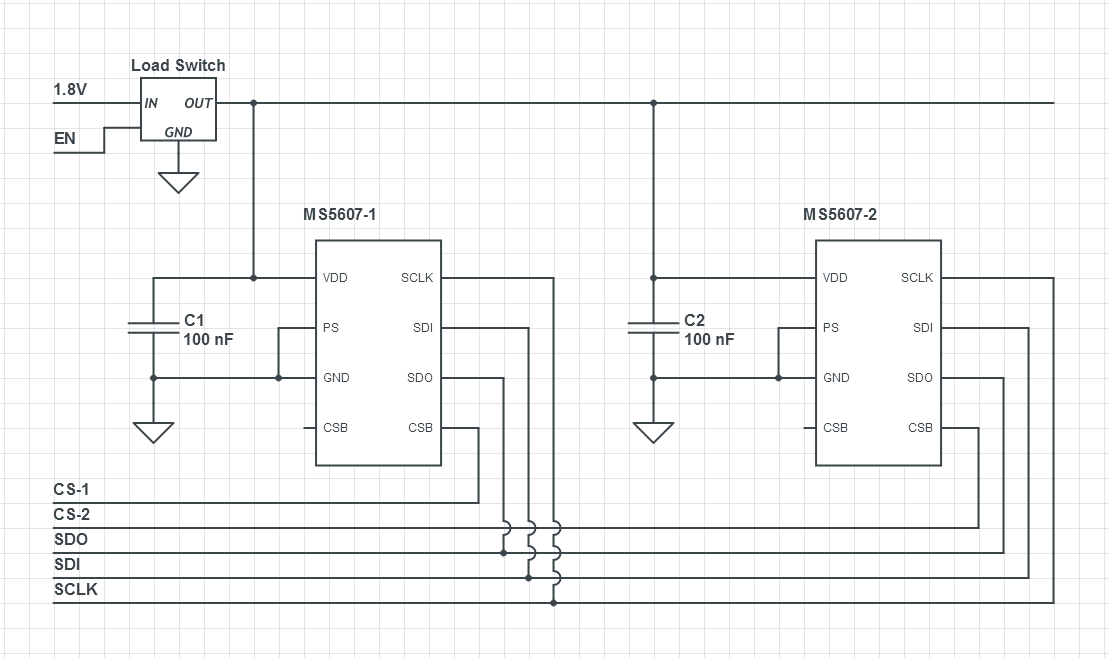
The tracker is expected to operate at altitudes above 10km. Because of that, MS5607 absolute pressure sensor with its extended range of 10hPa to 1200hPa (~31km ceiling) was chosen to provide the pressure readings from inside the balloon and of the surface of the PCB outside the balloon. The accuracy of the pressure measurements is stated to be +-3.5hPa with maximum resolution of 2.4Pa. The sensor can also provide temperature measurements with absolute accuracy of +-4.0°C in -40°C to 85°C range with maximum resolution of 0.002°C.
Both IC's will be powered through the same controllable load switch as the two thermistors and require a 100nF capacitor as close to the Vdd pin as possible. The SPI interface was chosen to establish the communication between the MCU and the sensors. The other option on offer was I
2C interface which on this tracker is level shifted and used to communicate with the transmitter. The conversion time with highest oversampling setting is stated to be 8.22ms at 1.4mA current consumption. $$dT=D2-C5 \times 2^{8}$$ $$OFF=C2 \times 2^{17}+(C4 \times dT) \; / \; 2^{6}$$ $$SENS=C1 \times 2^{16}+(C3 \times dT)\; / \; 2^{7}$$ Each sensor is factory calibrated and contains six coefficients (C1 to C6) stored in its non-volatile memory which must be read and used to compensate the pressure and temperature measurements. The full computation is rather lengthy and starts with calculating dT, OFF and SENS from the raw temperature output D2. $$TEMP=2000+dT \times C6 \; / \; 2^{23}$$ The datasheet states that to achieve accuracy over the temperature range, it is necessary to correct the temperature calculation (TEMP), the offset (OFF) and the sensitivity at actual temperature (SENS) by a second order correction factor: $$T2=dT^{2} \; / \; 2^{31}$$ $$OFF2=61(TEMP-2000)^{2}/ \; 2^{4}$$ $$SENS2=2(TEMP-2000)^{2}$$ For measurements where TEMP is less than 20°C. $$OFF2=OFF2+15(TEMP+1500)^{2}$$ $$SENS2=SENS2+8(TEMP+1500)^{2}$$ And further compensation for where TEMP is less than -15°C. $$TEMP=TEMP-T2$$ $$OFF=OFF-OFF2$$ $$SENS=SENS-SENS2$$ The compensated OFF and SENS values are then used to calculate the final pressure (P) from the raw pressure value (D1): $$P=(D1\times SENS \; / \; 2^{21}-OFF) \; / \; 2^{15}$$ The datasheet also provides charts for what I understand is a typical offset error caused by specific supply voltage choice. In case of 1.8V power supply, the temperature error is shown to be +0.38°C and the pressure error -2hPa.
Sensors - Ambient Light
I couldn't find a sensor that would operate at 1.8V and provide sufficient range for direct sunlight measurements. In the end, VEML6030 with 3.3V operating voltage was chosen to be part of the Si5351B circuit with which it would share the level shifted I
2C lines as well. This will add between 30ms to 110ms, depending on chosen integration time of the sensor, to the time the 3.3V boost converter is switched on.
The sensor itself is sensitive to 'close to human eye' spectrum and allows measuring ambient light from 0 to 120,000lux with resolution of 1.84lux. At 100ms integration time the current consumption is stated to be 45μA. $$y=6.0135 \times 10^{-13}x^{4}-9.3924 \times 10^{-9}x^{3}+8.1488 \times 10^{-5}x^{2}+1.0023x$$ As per application note:
Designing the VEML6030 Into an Application, the readings above 1,000lux will be corrected in software for the sensor's non-linearity using the equation above.
Sensors - Battery Voltage
Unlike the previous sensors, the battery voltage measuring circuit is continuously connected to the battery making it necessary to limit the current leaking through this path. Thus two 1MΩ resistors were chosen to form a voltage divider keeping the current between 0.45μA and 0.95μA. The resulting high source impedance (0.5MΩ) for the ADC meant that a 15nF capacitor was placed across the input again to provide a pool for the ADC's sampling capacitor (3.2pF) to tap into without dropping the measured voltage.

Since the measured voltage is connected continuously and by its nature fast changes aren't expected, the time constant (7.5ms) of the capacitor-resistors pair can be ignored. Figures on the order of gigaohms for insulation resistance of MLCC capacitors can be found which puts the additional leakage current through the capacitor to nano/picoamps. The 0.5% tolerance resistors alone should provide accuracy to a few millivolts. However, the actual readings will depend on the overall noise of the setup.
ESD Protection
While I was reading through some old #highaltitude
logs, I came across mentions of ESD presence on high altitude balloon trackers. Apparently, charge can due to air friction build up on an antenna endangering the RF input/output. Since at floating altitudes there is little to no humidity in the surrounding air, the charge can't effectively dissipate.


After looking into the subject more closely, I decided to add some protection. Namely, an ESD diode at the GPS module's RF input and a static bleeder resistor at the transmitter's antenna input. The ZOE-M8B's integration manual recommends to add a low capacitance (0.5pF) ESD9R3.3S diode as in the illustration above. While in case of the Si5351B's output, I decided to connect a 1MΩ resistor between the antenna's input and PCB ground to avoid detuning the low pass filter with any additional capacitance. The measures are intended to safely dissipate any ordinary charge build-up on the lines. They are not meant to protect against a storm. The balloon wouldn't most likely survive such encounter anyway.
Accessory Circuitry
Since there was some spare space on the PCB around the tracker as I went on to design it, I decided to add a snap-off piece with a couple of additional components to help with programming of the finished device. They are a 1.8V to 3.3V level shifter for the SWDIO and SWCLK lines, plus a current limited reset line on one side. And a 1.5V LDO to run the tracker from a LiPo battery during testing on the other side. This snap-off board is not part of the tracker itself and can be left out from the design.
Schematic
The actual schematic was drawn in the free version of Autodesk's EAGLE software which allows designing two layer boards of up to 80cm
2. So far, I have done all my designs in EAGLE.
For illustration, this is the main schematic window. I usually try to split the design into logical blocks to keep it easy to orient in. The SHOW tool is quite helpful in highlighting same signal traces as can be seen in the screen above. Properly naming and labelling signals that connect to parts in different blocks helps too.
This is the complete schematic of the tracker exported to a high resolution png file. It captures all the previously described circuits in their full and final form. This schematic then serves as the basis for the actual board design which can be entered by clicking 'Generate/switch to board' icon in the menu bar at the top.
Estimated Consumption
At this point, I will summarize the design's expected consumption using the maximum values provided by the datasheets. Later, these results will be confronted with actual measurements once the tracker is finished. The envisioned operation of the tracker is divided into four stages. Standby where the MCU is in its low power mode, and components that can be shut down are shut down. Active 1.8V corresponds to acquiring GPS positional fix and measurements from 1.8V sensors. Active 3.3V summarizes acquisition of ambient light measurement. And Transmitting maps the consumption during a 0.8s long transmission of an APRS packet. Each stage is complemented by an estimated duration.
|
t [s] |
TPS61099 |
SAML21 |
TCXO |
TPS3839 |
Vbatt |
| Transmitting |
0.8 |
3.1μA |
1.47mA |
1.5μA |
0.15μA |
0.95μA |
| Active 3.3V |
0.1 |
3.1μA |
356μA |
1.5μA |
0.15μA |
0.95μA |
| Active 1.8V |
3.0 |
3.1μA |
356μA |
1.5μA |
0.15μA |
0.95μA |
| Standby |
90.0 |
3.1μA |
1.5μA |
1.5μA |
0.15μA |
0.95μA |
First a summary of components that run continuously such as the main 1.8V boost converter, the MCU and its TCXO, the MCU supervisor, and the battery voltage divider. The MCU's consumption differs based on its state and operating frequency. Here it is at 4MHz in both active modes and at 12MHz with active DAC peripheral while transmitting.
|
t [s] |
MIC9407 |
ZOE-M8B |
MIC9407 |
Vtherm |
Vtherm |
MS5607 |
MS5607 |
| Transmitting |
0.8 |
1.0μA |
15.0μA |
1.0μA |
0 |
0 |
0 |
0 |
| Active 3.3V |
0.1 |
1.0μA |
15.0μA |
1.0μA |
0 |
0 |
0 |
0 |
| Active 1.8V |
3.0 |
9.0μA |
34.5mA |
9.0μA |
36.0μA |
36.0μA |
1.4mA |
1.4mA |
| Standby |
90.0 |
1.0μA |
15.0μA |
1.0μA |
0 |
0 |
0 |
0 |
This table contains components which are part of the two 1.8V circuits controlled by the two load switches. I've used the datasheet's 34.5mA current consumption of the Acquisition engine for the ZOE-M8B GPS module assuming the worst case scenario that the module has to run full power on every wake-up. In reality the consumption should mostly be the Tracking engine's 7.3mA. The duration of this stage is an estimate dictated by the GPS module based on my previous tracker that used MAX-M8Q to acquire positional fixes.
|
t [s] |
TPS61099 |
SI5351B |
TCXO |
FXMAR. |
VEML6030 |
| Transmitting |
0.8 |
4.1μA |
40.6mA |
2.5mA |
370μA |
0.5μA |
| Active 3.3V |
0.1 |
4.1μA |
35.0mA |
2.5mA |
370μA |
45.0μA |
| Active 1.8V |
3.0 |
1.6μA |
0 |
0 |
0 |
0 |
| Standby |
90.0 |
1.6μA |
0 |
0 |
0 |
0 |
The components supplied by the controllable 3.3V boost converter are summarized in this table. The ambient light sensor takes 100ms to take a measurement during which the whole circuit is powered (Active 3.3V). Later, it can be shut down, and the actual packet transmission can take place (Transmitting). During Active 1.8V and Standby stages the whole 3.3V circuit is powered down and the only consumption should come from the boost converter's shutdown current.
|
t [s] |
Effic.(1.8) |
Effic.(3.3) |
Total(1.8) |
Total(3.3) |
Total PWR |
| Transmitting |
0.8 |
91% |
88% |
1.5mA |
43.5mA |
166.0mW |
| Active 3.3V |
0.1 |
91% |
88% |
379.0μA |
37.9mA |
143.0mW |
| Active 1.8V |
3.0 |
92% |
70% |
37.8mA |
2.0μA |
73.9mW |
| Standby |
90.0 |
80% |
70% |
24.0μA |
2.0μA |
62.0μW |
The efficiency values come from TPS61099's datasheet and were derived from corresponding charts. The following columns summarize the total current consumption in 1.8V and 3.3V sections during different stages of operation while the last column shows the total estimated power consumption. Taking into account the durations of individual stages, the values presented above yield a 3.99mW average power consumption. The AAA Energizer Ultimate Lithium battery holds about 1.875Wh of electrical energy (1.25Ah * 1.5V). One such cell could power the tracker for 19.6 days. Increasing the delay between active states from 90s to 120s would see the duration rise to 25.7 days. In case of transmission every 3 minutes, 37.8 days could be achieved.
PCB Design
Once a schematic is finished, and EAGLE is switched to the Board window, the shape of the actual PCB can be outlined, the components arranged, and all the traces connecting them drawn, so an actual board design can be sent to a manufacturer.
This is what the work area in EAGLE looks like. All the parts from the schematic with their respective connections highlighted are laid down next to an outlined shape of a board. The free version of EAGLE allows placing components and routing traces on the Top (red) and Bottom (blue) layers of a PCB. Doing more complex designs (4 or more layered, larger boards) requires paying a subscription fee for higher versions of the software.
There are limitations to how thin a trace or small a distance between traces a manufacturer can make. These design rules are usually summarized on the manufacturer's website. I've been using OSH Park to have my boards made for some time now and intend to order this board from them as well. Hence the specifications from the screen above are respected in the design described in the following paragraphs. Aside from the design rules, there are additional documents in the OSH Park Docs section that may shed light on some of the terms and help with the design.


EAGLE is distributed with numerous libraries which contain individual components stored in terms of a Symbol and a Package. A Symbol, as seen in the image on the left, belongs on a schematic and lets the user wire individual connections between the component and other parts. A package, in the image on the right, then specifies the precise dimensions of copper plating, openings in solder mask, or drawings on silkscreen, and goes on the actual board. The in-built libraries don't contain all imaginable components, so I usually design the symbols and packages myself following recommendations from the component's datasheet.


Since this tracker hosts a number of ICs in quite tiny and high pitched packages, some of them might be at odds with the manufacturer's limits. To illustrate what I mean, this is a comparison of a design and an actual board containing a few 0402 packages for small resistors and capacitors, and two tiny voltage regulators in an X2SON package (1x1mm). The board works, but it seems that for example by choosing the trace widths to the X2SON package more carefully, the manufacturer might find it easier to make the copper pads more uniform.
Once I have the PCBs and components, I intend to use my
reflow oven to solder them together. To do it properly, I will be ordering a stencil which allows depositing precise amounts of solder paste to each pad on the board. The stencil can be designed in EAGLE as well by including the Cream layer in package designs as can be seen in the image above. This is a portion of the MCU's package where the red areas represent the copper layer (Top layer), the hatched areas outside the copper pads correspond to openings in a protective solder resist (tStop layer) which covers the naked copper layer on a finished PCB. While the hatched areas inside the copper pads outline openings in the stencil (tCream layer).

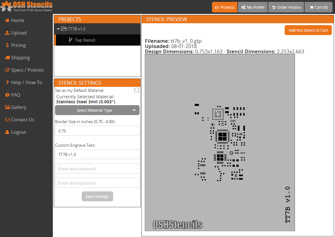
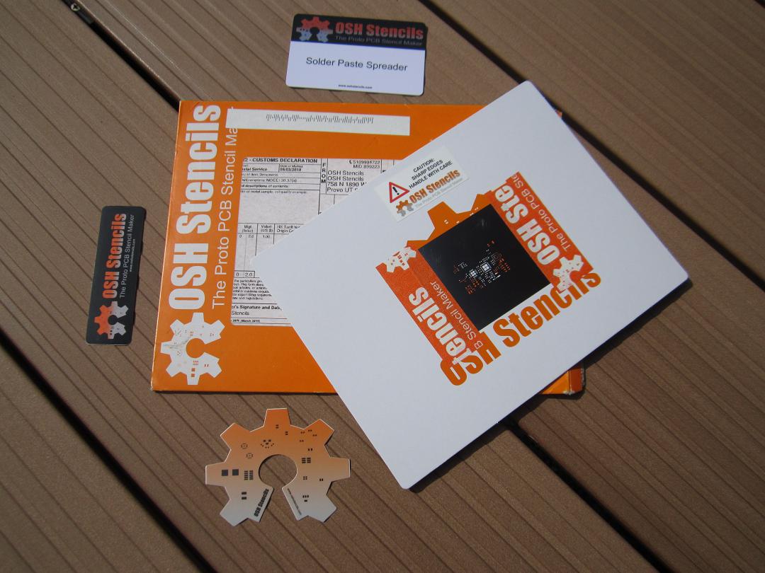
My intention is to order from OSH Stencils who offer stainless steel stencils in 3-8mil (76, 102, 127, 152, 178 and 203µm) thicknesses with minimum aperture size of 25.4µm and a minimum laser spot size of 17.8µm. Aside from these limits there are some guidelines on choosing the stencil thickness and soldering paste type based on the packages being soldered. I've sourced the information from Indium Corporation's
Powder Choice Stencil Design Guidelines document. The aim of these guidelines is to ensure the soldering paste gets deposited on the PCB and doesn't stay inside the stencil. $$Area\;Ratio=\frac{D}{4t}\qquad\qquad Area\;Ratio=\frac{LW}{2t(L+W)}$$ To achieve that, an aperture in the stencil should have the $Area\;Ratio$ larger than 0.66. The ratio is the area of the aperture opening divided by the area of the aperture walls. Soldering pastes on the market differ in grain size, in other words, how small the largest particles are. The guideline states to choose such a paste that 4-5 particles can fit across the aperture. Calculating these values for all components on the tracker, a Type 3 paste (25-45µm particle size) could be used with a 76µm stencil.


Provided the whole content of an aperture gets deposited on a PCB, the volume of the paste equates to the aperture area times the stencil thickness. What I couldn't find addressed anywhere was whether there is a minimum required volume of solder paste for a proper solder joint. Because the difference in volume between different thicknesses may be significant. Anyway, when drawing the packages, I mostly followed recommendations from datasheets if present. If not, I applied a suggestion from NXP's
AN1902 application note to make the stencil openings a minimum of 25µm smaller than the copper pads. In a couple of cases, I thought OSH Park may have problems reproducing small circular pads and solder mask openings, so I diverged from the recommended shape and made them more squarish.

A finished PCB is covered with a solder mask. This polymeric layer has openings around each pad and helps with avoiding solder bridging between adjacent pads. In some cases, however, the distance between individual pads is quite small. OSH Park, for example, requires 102µm minimum thickness of a solder mask web. Otherwise, the board is manufactured without it between the pads that are too close. On the other hand, OSH Park also recommends to expand the mask around pads by 51µm to account for fabrication tolerances - the mask may be shifted a little to a side. In a few instances, such as the FXMAR2102 above, the pads were too close, so I had to decrease the expansion to only 25µm to ensure the mask gets printed between them as well. This means that in case the mask is shifted, it may cover a little bit of the pad.


In the actual design, I use ground planes on both sides of the board to serve as the return path for currents from individual components - as opposed to wiring each ground connection separately. The top plane gets fractionated by the components and most of the traces a lot while I try to limit the number of traces splitting the bottom plane. In EAGLE, ground planes are created by drawing a polygon around the board outline and assigning it to the GND signal as in the images above.

At the beginning, I arranged the components inside a basic board outline according to what made sense for its intended use. A tracker generally hangs underneath a balloon, so the transmitter was placed at the bottom of the board where an antenna extending down from the tracker can be attached close to the IC. The microcontroller having the most connections to the rest of the components was placed roughly in the middle. It was oriented to make the traces to the respective peripherals as short as possible. A programming tab extended to the left of the MCU. This expanded space was also used for the GPS chip antenna's rather large clearance area which put the GPS module to the left top corner. The power supplies were focused to the right side of the board. Since I intended to extend a couple of external sensors to the balloon itself using wires, the sensor circuits including pads for the wire connections were placed in the top right corner.


Once I had a basic idea of where individual components would be, I began the actual routing. Some datasheets or application notes provide an example layout for the component. This, for example, is the boost converter TPS61099 as laid out in figure 29 of the datasheet in the image on the left and an actual layout I did on the tracker inspired by the example shown in the image on the right.
Mostly though, datasheets provide only rough guidelines such as
'a 100nF ceramic capacitor must be placed as close as possible to the Vdd pin' and leave the layout up to the designer. That opens up a wide variety of ways to connect the components to each other. An actual trace on a pcb has some resistance, capacitance and inductance depending on its dimensions, dimensions of the pcb and the signal's return path (more
details). There are calculators and software to model or approximate specific situations, but aside from a couple of special traces - carrying RF (more on that later), I got by with a much simplified approach of using the thinnest trace width OSH Park could manufacture for data lines, while widening the power carrying traces to decrease their impedance.
Another aspect I tried to keep in mind was that the frequency of a signal determines the path current will take when returning through the ground plane. A DC signal will return via a path of the least resistance which is typically the physically shortest path on a ground plane. On the other hand, an AC signal will follow the path of the least impedance which means that the returning current in the ground plane will try to follow the path of the trace on the top layer. A visualization of these principles can be found
here. In case the path is blocked and the return current is forced away from the top layer trace, the circuit encloses a larger loop area which increases the induction of the path, the loop radiates more power, the carried signal is more susceptible to interfering signals, and as a result of uncontrolled currents flowing around, the ground plane may be at different potentials - an explanation of ground bounce phenomenon
here. What this all meant in the design itself was that I tried to ensure there were, if possible, straight paths for the return currents on the ground plane. In the end however, the lack of space became the dominant factor and splitting the bottom ground plane and extending the return paths became necessary. It most likely won't lead to any catastrophic failures, but it may mean increased noise in the system and analog measurements. Passing EMC regulations for commercial production with this design is also unlikely. In the end, even TT7F didn't take these actualities into account and managed to serve its purpose.
To illustrate what was mentioned in the previous paragraph, this is a part of the board with the microcontroller's VDDANA supply and the main 1.8V boost converter. According to
this Maxim Integrated's document, the MCU's immediate high frequency current demand is satisfied by the nearby 100nF bypass capacitor (the current flow marked by the green arrows) since the source of the power supply may be too far to provide the current without dropping the voltage. The other current loop (blue) then serves to supply the low frequency or DC currents. As can be seen in the image, the returning DC current (dark blue) can't flow in straight line and has to find a way around the trace cutting the ground plane.
These three images highlight the power supply wiring as carried out in the design. The image on the left shows the battery input at the top right side close to the main 1.8V boost converter. A separate pad right next to the battery input pad allows soldering on jumper leads for manually turning the tracker on and off. A wide trace delivering the battery input to the 3.3V boost converter in the right bottom corner runs along the edge of the board as does a parallel path on the ground plane. An uncovered ground pad underneath the second converter serves as a connection to the battery's negative terminal. The middle image shows the main 1.8V power supply with both of its load switches. All components on the line have their 100nF decoupling capacitors quite close to their respective VCC and GND pins, but the ground return path back to the source converter is much less ideal, usually cut by a few traces along the way. Something similar could be written about the 3.3V power supply in the image on the right. Although the ground plane is much less cut in this case, and the furthest reaching 3.3V arm won't most likely carry much current since it supplies three unused outputs of the Si5351B.


The GPS ceramic chip antenna itself is quite small (3.2 x 1.6 x 1.1mm), but the recommended layout (in the image on the left) requires a 4.00x6.25mm clearance area without any metal. I decided to achieve that by extending the board by a 6x8mm piece of material in the top left corner. Otherwise, I tried to follow the datasheet's layout.
As mentioned in the schematic section, I left myself an option to choose how I supply the GPS module's backup circuitry. The decision is made when soldering a 0
Ω resistor to R15 which is a two way package connecting the backup power supply pin to either the same load switch controlled 1.8V supply as the rest of the IC, or the the main always active 1.8V power supply. The former option cuts the GPS module completely off while the latter option (shown in the image above) supplies the backup circuitry when the load switch is turned off.

The top right corner of the PCB hosts the on-board pressure sensor, while the bottom layer provides six 2x1mm pads for soldering wires to the external pressure sensor (pad description in the image above). The leads of the on-board thermistor can be pushed through two larger unmasked vias (drill diameter 0.3302mm) and soldered directly to the board. The thermistor bead can extend up to 45mm from the PCB. Two 2x1mm pads for soldering wires to the external thermistor are located next to the vias on the bottom layer. The image also shows the positive battery input terminal located right next to an isolated pad which can be used for an on/off jumper.
The traces carrying RF signals to the GPS receiver and from the transmitter output were designed to match to a 50Ω impedance. The transmission line type is called grounded coplanar waveguide and is illustrated in the image above.
This online calculator was used to arrive at 0.791mm trace width with 0.1524mm gaps between the adjacent ground planes and the signal trace. The calculation further assumed a 0.8mm thick PCB, 70µm copper layer thickness and relative dielectric constant of 4.6. Vias connecting the top and bottom ground planes were placed along the signal trace to provide path to return currents induced on the top layer (according to Maxim Integrated's
General Layout Guidelines for RF and Mixed-Signal PCBs). Where a gradual bend was not possible, a mitered right-angle bend was designed according to an equation in the same document.
Because of the proximity of the 3.3V boost converter to the transmitting antenna, I thought it may be better to separate their grounds. A 1mm gap in ground planes on both sides of the PCB encloses the boost converter currents separating them from the antenna pads and the filtering network. If I try to visualize the currents at play, maybe the vias surrounding the two blocks would do the job anyway. I also can't recall seeing any other designs doing it this way. Anyway, this is how the design was carried out. The image also shows the TCXO surrounded by ground vias to contain its high frequency currents. Although, the level translator's DC return path may lead right underneath the oscillator.
The programming tab contains five signals for a SWD programmer/debugger ordered as described in the image above. The VTref signal (target voltage sense) is connected to the MCU's VDD pin - 1.8V. The form of the connector was inspired by
this approach. The 1mm pitched pads were designed to mate with a cut (5 pins) PCI Express connector. Alternatively, leads can be soldered directly to the tab. Before launching the tracker, the tab can be snapped off along the thinner section demarcated by the line of holes in the material.

As mentioned previously, the GPS antenna clearance area expanded the board to the left by a few millimeters. I decided to utilize the space that arose and added another snap-off piece which carried another level translator at the top and a 1.5V LDO at the bottom. Originally, there was only a 1mm wide slot between the tabs. However, it occurred to me I should have asked OSH Park about the size of the tool they use to mill the board outline. The response was that they typically use a mill end that is 1.73mm in diameter, and recommend slots of at least this width. But they also have a 1mm mill end available so that 'should' work. Nevertheless, since it wasn't constraining my design that much, I widened the slots to 2mm.

This is the finished board design. The yellow lines (tDocu layer) typically outline the actual dimensions of the package for information purposes and won't be part of the manufactured board. Aside from the accessory snap-off tab, all components are located on the top layer. I didn't put too many markings on the silkscreen layers (tPlace, bPlace) to let the board look cleaner, at least to my eyes. Usually just labelling the first pin to help orienting the component. So if anyone intends to build this tracker, they will have to know the board when populating it. The description here is quite extensive, I think.


This is an evolution of the design for illustration. Starting with a basic idea and initial component arrangement, I went on wiring the components from the transmitter and the 3.3V boost converter at the bottom to the components along the right side of the board (top view), finishing with the microcontroller. The GPS module and antenna were fixed in their position quite early into the design as well. I had to expand the board a little along the way as it became clearer that some bits may be hard to fit. Individual images were rendered by OSH Park upon uploading the design to their website.
These are also images by OSH Park of the finished board that capture individual copper pours. It's apparent that the bottom ground plane ended up quite scarred by traces. Some of the return currents, especially between the pressure sensor and the MCU, will be forced quite a distance from their forward flowing counterparts.
Ordering
At this point, it was time to send the design to a manufacturer, order components and everything else needed for assembling the boards. It turned out that most of the orders would be placed with US based companies - OSH Park for the boards, OSH Stencils for the stencil, and Mouser for the components. Despite being on the other side of the world, it currently is the most cost and availability effective solution for me. Although, it does mean a bit longer delivery times.

Ordering the boards is easy. It requires only uploading the design (.brd file) to the OSH Park website, filling in the mailing address, and paying with a credit card. The cost depends on the dimensions of the board - calculated as the smallest rectangle encompassing the design. I opted for the 2oz copper with 0.8mm FR4 thickness service for \$5.25 per three boards - the PCBs were 20 x 34mm. And I chose the free International First Class shipping without tracking. The boards took 14 days to deliver to the Czech Republic. Out of that, 9 days were spent on the fabrication according to OSH Park.
This is a screenshot of EAGLE showing only the tCream layer which serves as the basis for manufacturing a stencil. All the outlined areas demark spots where soldering paste should be deposited on the boards when populating the tracker with components.
Ordering the stencil is similar to ordering the PCBs. After uploading the .brd file to OSH Stencils' website, choosing the material, stencil thickness and dimensions, the site calculates the cost. Payments can be made via a credit card. I chose a 76μm (3mil) thick stainless steel stencil 57 by 68mm in dimensions. For that I paid the minimum order of \$10 plus \$7.93 for shipping to the Czech Republic with USPS (International First Class with tracking). The stencil was shipped the next day and delivered after 26 days since ordering.


As I mentioned, I use the big distributors' online catalogues to choose and look for components. To my knowledge, it is also the easiest way of obtaining the more specialized parts in the Czech Republic. For this project, I ordered almost all components from Mouser. The one exception was the u-blox ZOE-M8B module which I got from a local distributor. If the price of an order is above €50, Mouser ships the package with Fedex without any additional payment for the delivery. Fedex provides tracking, so occasionally the parcel can be followed on its route. Here it is arriving in Europe. It was delivered from Mansfield, Texas to Roznov pod Radhostem in the Czech Republic in 5 days 10 hours.
| # |
Part Number |
€ |
# |
Part Number |
€ |
# |
Part Number |
€ |
| U1 |
SAML21E17B-MUT |
3.33 |
R1 |
SFR01MZPF1504 |
0.081 |
C6 |
GRM155R60J106ME15D |
0.177 |
| U2 |
ZOE-M8B |
11.64 |
R2 |
SFR01MZPF1504 |
0.081 |
C7 |
GCM155R72A222KA37D |
0.069 |
| U3 |
FXMAR2102UMX-F106 |
0.47 |
R3 |
CRCW04021M87FKED |
0.045 |
C8 |
CC0402JRX7R6BB104 |
0.011 |
| U4 |
520L15IA26M0000 |
3.38 |
R4 |
RC0402FR-131KL |
0.011 |
C9 |
CC0402JRX7R6BB104 |
0.011 |
| U5 |
CM8V-T1A-32.768kHz-7 |
0.77 |
R5 |
RC0402FR-07649KL |
0.011 |
C10 |
GRM155R71E183JA61D |
0.103 |
| U6 |
MIC94070YMTTR |
0.48 |
R6 |
ERJ-2RKD1004X |
0.053 |
C11 |
GRM155R60J106ME15D |
0.177 |
| U7 |
MS560702BA03-50 |
2.75 |
R7 |
ERJ-2RKD1004X |
0.053 |
C12 |
CC0402JRX7R6BB104 |
0.011 |
| U8 |
LSF0102DCUR |
0.61 |
R8 |
RR0510P-4992-D |
0.040 |
C13 |
CGA2B2X5R1E153K050BA |
0.024 |
| U9 |
NCV8114ASN150T1G |
0.39 |
R9 |
RR0510P-4992-D |
0.040 |
C14 |
CGA2B2X5R1E153K050BA |
0.024 |
| U10 |
W3011A |
1.71 |
R10 |
RC0402FR-131KL |
0.011 |
C15 |
CGA2B2X5R1E153K050BA |
0.024 |
| U11 |
SI5351B-B-GM |
2.74 |
R11 |
ASC0402-100KFT10 |
0.024 |
C16 |
CC0402JRX7R6BB104 |
0.011 |
| U12 |
TPS3839G18DQNR |
0.65 |
R12 |
ASC0402-100KFT10 |
0.024 |
C17 |
CC0402JRX7R6BB104 |
0.011 |
| U13 |
MIC94070YMTTR |
0.48 |
R13 |
ASC0402-100KFT10 |
0.024 |
C18 |
CC0402JRX7R6BB104 |
0.011 |
| U14 |
SIT1552AI-JE-DCC-32.7 |
2.20 |
R14 |
RC0402FR-074K7L |
0.010 |
C19 |
C1005X7S0G105M050BC |
0.057 |
| U15 |
VEML6030 |
1.96 |
R15 |
AC0402JR-070RL |
0.013 |
C20 |
GRM155R60J106ME15D |
0.177 |
| U16 |
TPS61099YFFR |
1.55 |
R16 |
RC0402FR-074K7L |
0.010 |
C21 |
CC0402JRX7R6BB104 |
0.011 |
| U17 |
TPS61099YFFR |
1.55 |
R17 |
RC0402FR-074K7L |
0.010 |
C22 |
CC0402JRX7R6BB104 |
0.011 |
| U18 |
MS560702BA03-50 |
2.75 |
R18 |
RC0402FR-074K7L |
0.010 |
C23 |
C1005X7S0G105M050BC |
0.057 |
| T1 |
PX502J2 |
2.08 |
R19 |
ERJ-2RKF39R0X |
0.022 |
C24 |
C1005X7S0G105M050BC |
0.057 |
| T2 |
PX502J2 |
2.08 |
R20 |
CR0402-JW-204GLF |
0.011 |
C28 |
GRM155R60J106ME15D |
0.177 |
| D1 |
ESD9R3.3ST5G |
0.55 |
R21 |
ERJ-2RKD1004X |
0.053 |
C29 |
GJM1555C1H200FB01D |
0.167 |
| L1 |
LQW15AN56NG00D |
0.20 |
C1 |
CC0402JRX7R6BB104 |
0.011 |
C30 |
GJM1555C1H200FB01D |
0.167 |
| L2 |
BLM15PX471SZ1D |
0.17 |
C2 |
CC0402JRX7R6BB104 |
0.011 |
C31 |
CC0402JRX7R6BB104 |
0.011 |
| L4 |
VLS201610CX-2R2M |
0.45 |
C3 |
CC0402JRX7R6BB104 |
0.011 |
C32 |
GRM188R60J226MEA0D |
0.299 |
| L5 |
MLP2520W1R0MT0S1 |
0.45 |
C4 |
CC0402JRX7R6BB104 |
0.011 |
C33 |
GRM188R60J226MEA0D |
0.299 |
| PCB |
20x34x0.8mm |
1.53 |
C5 |
CC0402JRX7R6BB104 |
0.011 |
BAT |
ENERGIZER L92 |
1.950 |
These are all the components necessary to build the tracker. The marking corresponds to the marking as used in the EAGLE schematic. A number of components, especially the capacitors and resistors, can be replaced with alternatives. These components are simply the ones I ordered mostly from Mouser, hence the prices I paid for them are included. The total cost per one tracker taking into account only the components is about €52 (stencil, soldering paste, etc. not included).
Assembly
Once all the packages had arrived, it was time to check everything up and prepare for the reflow process. This was going to be my first proper attempt reflow soldering and straight away on a quite expensive board. For that reason, I intended to do a couple of tests before I dived in with the full assembly.
All components were packed separately in anti-static or dissipative packaging depending on the needs of the specific part. I've noticed that on a few occasions whomever handled the order had added a couple more units of the component than was ordered. The circuit boards usually arrive in a somewhat rough state and bits and pieces at the edges need to be filed off.
The stencil arrived in a solid board envelope with a plastic credit card shaped solder paste spreader and a couple of stickers. I had to order the soldering paste from a local seller, because a lot of the mainly chemical stuff that Mouser have on offer is not shipped to the Czech Republic - due to some transport regulations, perhaps? The paste I got was a syringe of a no-clean leaded Sn62Pb36Ag2 based Type 3 (25-45µm particles) soldering paste labelled as ESN62PB36AG with a melting temperature of 179°C.
Here are a few detailed photos of the actual boards. Even the smallest pads seem both visually and electrically ok. A closer look at the X2SON package (TPS3831) suggests that, indeed, widening of the tracks leading to pads results in a much more uniform shape of the actual copper pours.
Since the PCBs were much thinner than those I had already tested in my
reflow oven, I wanted to know what that would mean for TT7B boards in terms of temperature. Similarly to the tests I did when constructing the oven, I taped the thermocouple to one of the boards, placed the board on top of two spacers, and ran a profile for leaded pastes (more details on testing the oven in the link above). The TT7B board has half the volume of the small PCB from previous tests. Unsurprisingly, it heats up faster and peaks at 233°C which is still safely within the limits.
Speaking of limits, the maxima and recommended soldering conditions are usually described in a components datasheet. In case of components populated on TT7B, most of them simply reference
JEDEC J-STD-020C standard which provides specific boundaries on the temperature levels, ramp-up/down rates, and durations of individual phases of a reflow profile (further details about the illustration above can be found in the document itself). Some of the more sensitive parts then mention additional restrictions such as the peak temperature must not exceed 255°C in case of ZOE-M8B, or the MS5607 should be soldered with 62%Sn36%Pb2%Ag paste rather than 63%Sn37%Pb. All in all, the temperature profile for leaded soldering pastes programmed in my reflow oven should adhere to these limits.
A more detailed look at the stencil. Despite knowing the dimensions, only after I had the stencil in my hands, it pointed out to me how tiny some of the apertures were. It was, though, nice to see that even the tiniest holes were precise in shape.
Before depositing the soldering paste, I used old spare PCBs and a masking tape to fix the TT7B board in place - an approach one can see in many tutorials and Youtube videos. One slight adjustment I had to make was to bolster the board with another one, because the TT7B was 0.8mm thick while the surrounding PCBs were thicker - 1.6mm. This helped the stencil, after it was aligned and secured in place, to abut against the board without excessive hogging or sagging when pressed.


The soldering paste is stored in a fridge and should be left to warm up to room temperature prior to depositing it on the board. I also emptied the syringe to a small plastic container where it could be properly stirred. Typically, I deposited a bit of paste in a line along the left side of the apertures. Then squeegeed it across the apertures left to right holding the credit card spreader at a low angle pressing against the stencil. Holding the spreader perpendicular to the stencil and doing the same clears the excess paste off the stencil. In case some of the apertures didn't get filled the first time, I used the excess paste and squeegeed over them again. This in principle sounds easy and a number of Youtube videos suggest it is, however my experience was much less ideal. I don't know whether it was because of the paste I used, incongruousness of my approach, or difficultness of the design, but usually portions of the board were printed nicely while the rest was too liquidy meaning the individual deposits didn't hold shape and spilt into each other. This started a repeated cycle of cleaning the PCB, stencil and spreader with isopropyl alcohol, realigning the stencil, squeegeeing the paste in another attempt, removing the stencil and finding a poor result once again, wiping the excess paste and storing it for future use. In the end, somewhere between the 10th and 15th attempt, the paste printed in such a way that I was willing to risk it and go through with the rest of the process. The image above shows the state of the paste I actually used to reflow the board. The liquid paste is apparent especially at the SAML21 and Si5351B footprints.

The datasheet states that 'the paste doesn't lose its physical and chemical properties even after being left for 20 hours on the PCB'. This turned out to be handy, because it took me about two hours to place and orient all the components. I did it with a pair of anti-static tweezers and a wooden tooth-pick for the more delicate aligning.
In contrast to the previous steps, the actual reflow took a little over five minutes and was quite uneventful. I used the same profile for leaded pastes as in the test conducted earlier, and the board was laid on top of two spacers to thermally decouple it from the large aluminium plate.
This is a higher resolution image of the finished board. There is some soldering paste residue visible on the larger pads which probably escaped the repeated cleaning after each attempt to print the paste with the stencil. It doesn't, though, seem to actually corrupt any connections on the board. A few of the smaller components ended up aligned a little crooked, but all the big ones stayed nice in place.
These are a few close-ups of some of the reflown solder joints. I was pleased to see the two large QFN packages (SAML21, Si5351B), which had the paste printed a bit liquidy, to form nice connections without any bridging all around the package.

The very first powered check I did on the board was using the accessory 1.5V regulator to power the tracker, and measuring the input current. It was in the realm of a couple hundred microamps which seemed presumable and ruled out any shorts. I then proceeded to check a few voltages around the board and found the MCU's reset line at only 0.7V. A closer inspection revealed the TPS3839 MCU supervisor hadn't reflown properly. In the image of the board with the printed solder paste, it can be seen that the paste in this footprint was also too liquidy which caused it to accumulate at one corner of the IC lifting it up and failing to create a proper connection. I intended to correct this with a hot air gun, but unfortunately as I tapped the IC to help it settle, I managed to took it off completely. Instead of making the situation possibly even worse, I decided to leave this tracker without the supervisor for the time being, potentially trying to solder it back at some point later. After this, the main voltage on the board was measured at 1.826V, the reset line at 1.754V, and the current flowing from the 1.5V regulator at 182
μA (measured with
μCurrent).
The mass of the populated tracker without the accessory tab is 1.56g (1.76g with the tab). Some extra mass is expected when the external sensors and an antenna are attached. The image on the right then shows a size comparison between my previous tracker TT7F, the TT7B, and a AAA Energizer Ultimate Lithium battery.
Programming
In the past, I got used to simple means of programming a microcontroller such as needing just a USB cable when programming Arduinos and the SAM3S on my TT7F, or using another Arduino to program a stand-alone ATmega328p. This time as I learnt, I would have to do the programming via SWD interface, and for that I would need an external programmer/debugger. I wasn't too keen on buying an expensive programmer (such as Atmel-ICE) to do just a couple of boards. The problem was that I couldn't find any low cost (Ebay clones) devices which could program Atmel/Microchip ICs - there were plenty for ST microcontrollers. The solution I went with in the end was hinted at in a few discussion forum posts. Apparently, a number of Atmel's evaluation boards were equipped with an additional IC which served as an external programmer/debugger that could be exploited. The following paragraphs describe how I do the programming. Anyone in possession of Atmel-ICE or a comparable device needs to just connect appropriate signals to the programming tab and program the tracker the usual way.


I chose the cheapest option that I could find which was a SAMD10-Xplained-Mini evaluation board for €10.37. Aside from the SAMD10 microcontroller the board is populated with an ATmega32U4 with a USB interface flashed with firmware that allows it to access the target MCU via the SWD interface. This embedded debugger (mEDBG) was what I intended to use. To connect to TT7B, I would utilize a modified PCI Express connector to mate with the programming tab as mentioned previously.
Since the SWD interface was connected between the two ICs, there were a couple of modifications that had to be done. The original image from above comes from
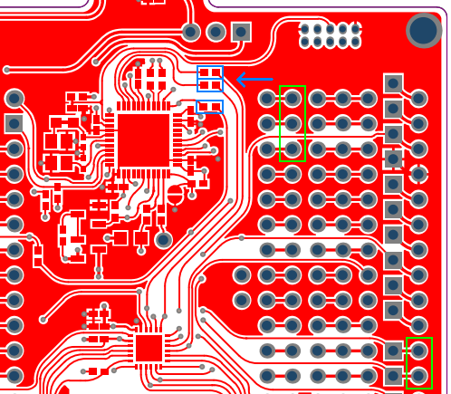
SAM D10 Xplained Mini Design Documentation which also contains a detailed schematic. After a little bit of study, I decided to desolder three SMD resistors outlined in the blue rectangles (R110, R111 and R112) and bring out the signals to three nearby pins (upper green rectangle). This broke the connections between the ICs on the SWDIO, SWCLK and TARGET_RESET lines. The three pins then provide direct access to the signals on mEDBG's side. In case I still wanted to use the SAMD10 for something, I could externally re-connect the lines to the two pins in the bottom green rectangle and a reset pin which is part of the SPI interface (at the bottom of the board not shown).


These photos capture the modifications I did on the board. After actually acquiring the board and some probing on the SWD lines, I found that the Target_Reset line wasn't just an open drain output, but once the mEDBG performed a reset, the line stayed at 3.3V. This meant that I would have to somehow level shift it as well. In the end, the solution I came up with required a PNP transistor and a resistor (more on that below). I also added a pin for external connection which is pulled up to 3.3V by a 3.3k
Ω resistor. This was to pull the Target_Reset line to Vcc, because the original pull-up was on the SAMD10's side of the disconnected programming interface. Due to this the Target_Reset line was low at power-up and required the first mEDBG reset to get and stay high. The RST and GND pins on the left side of the board then allow, when shorted, to force a manual reset of the target IC (the SAML21 in this case).
This solution for level shifting the Target_Reset line required the least number of components which was why it was chosen. The cost of this setup is that the PNP transistor doesn't bring the SAML21's Reset line (which is internally pulled up to Vcc) all the way to ground, but leaves it at about 0.67V for the period of the reset pulse - see the screenshot above (yellow - mEDBG's Target_Reset, red - SAML21's Reset). The SAML21's input High minimum threshold is stated to be 0.7*Vdd which equates to 1.26V, so it should be fine.


Another important piece is the accessory level shifter used on the SWDIO and SWCLK lines to translate the programmer board's 3.3V signals to TT7B's 1.8V, and vice versa. The SWCLK signal is only one way and driven by the mEDBG IC, so the pull-ups aren't populated - there already is a 1kΩ pull-up on the actual TT7B board as required by the datasheet. The SWDIO line, though, is bi-directional and the nature of the level shifter IC requires a pull-up on either side of the line - these are populated on the accessory board. In case of the PCI Express connector, it turned out that if I cut it where the 7 pin part separated from the 11 pin part, the smaller piece fitted precisely on the programming tab squeezing between the tab and the GPS antenna.


The TT7B board, however, was too thin, so I had to pad the insides of the connector with a few pieces of cut and straightened heat-shrink tube. After that the programming tab slid in precisely
where the contacts were. The signals were brought out at the back side of the connector where I soldered five pins for respective wires fitted with crimp sockets.


This is then what the whole hardware train looks like when programming the TT7B tracker. The target is powered from the accessory 1.5V regulator and a LiPo battery. The connector is slid on the programming tab extending the 1.8V (red), SWCLK (blue), SWDIO (green) and GND (black) signals to the accessory level shifter. The same signals from the high side of the level shifter then lead to respective pins on the programmer board. The RESET signal (white) connects directly to the emitter of the PNP transistor on the board. The SAMD10 Xplained board then connects to a PC via a USB interface. When I probed the connector side signals with the target board disconnected and the programmer board powered, the voltages appearing on the signal lines lacked the reference voltage and were around 2.4V. Because of this, when I program the tracker, I first power the TT7B board and then the programmer. Although doing it this way, the PNP transistor pulls the SAML21's Reset line down to 0.67V and holds the MCU in reset until the programmer is powered as well and 3.3V appear on the Target_Reset line.

This is an illustration to summarize the SWD interface in one place. The Target_Reset signal originates in the mEDBG's PD4 and PE6 pins which are most likely push-pull outputs. The signal connects to the base of a PNP transistor which switches on when the base goes low. When switched off (base is high) the SAML21's Reset signal is pulled high by an internal pull-up. The SWCLK clock signal is generated by the mEDBG's PB1 pin. The LSF0102 is a switch which conducts when either of the sides (An or Bn) is low, and presents high impedance when both sides are high. Since the SWCLK signal is unidirectional, the mEDBG's side is driven by a push-pull output while the SAML21's side requires a pull-up for when the switch is high impedance. The SWDIO signal is bi-directional, and as such the mEDBG's PB2 pin and SAML21's SWDIO pin alternate between being push-pull outputs and high impedance inputs. Because of that, both sides require a pull-up resistor.


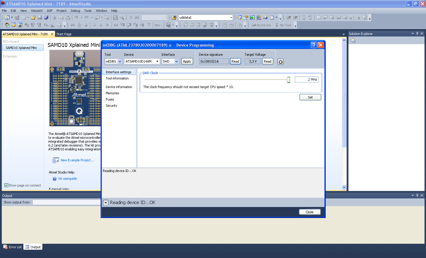
When the programmer board with TT7B is connected to the PC, Atmel Studio 6.2, which is what I use to write code and program the device, recognizes the Xplained Mini evaluation board. Upon clicking on Device Programming in the Tools menu, the Tool selection offers the recognized mEDBG, however the Device selection is fixed to the expected ATSAMD10D14AM microcontroller. An attempt to read the target device signature then pops up an info window about an unexpected device signature 0x1081021A (signature of SAML21E17B), and the software doesn't establish a connection to the MCU. To get round this, I modified the ATSAMD10D14AM.xml file located in 'devices' subdirectory of the main Atmel Studio installation. The modification consisted of replacing the content of the file with contents of ATSAML21E17A.xml file located in the same subdirectory. However, since TT7B is populated with a B version of the IC while the A version is 'Engineering Samples Only' according to the datasheet, I had to change the device name to ATSAML21E17B and the signature to 0x1081021A in a couple of places inside the file. After that the software was able to establish communication with the target, read the flash memory, read fuses, program the device, etc.


To program the target device, I select the 'Memories' tab, fill in the path to the compiled .hex file, and click 'Program'. The programmer then erases the target's flash memory, reprograms it with the desired code, and verifies the written content. In this case, it was a simple piece of code to verify the process and check the tracker's basic functionality. One by one, the code enabled the two load switches for a period of time while I measured the trackers consumption and voltages at respective points. The tracker passed this test successfully, so I can begin writing the firmware. More on that perhaps in a future blog post.
Downloads
For anyone interested in using any of the stuff described in this blog post, here are the Eagle schematic and board files, the Bill Of Materials, the modified XML file for Atmel Studio, and a link to a Github repository of this project.
TT7B's
schematic from Eagle.
TT7B's
board design from Eagle.
TT7B's
BOM export from Eagle.
Modified
ATSAMD10D14AM.xml for Atmel Studio.
Github
repository link.